

Rechercher


Accueil > La Recherche > Axes & Equipes > Physique Appliquée > Transport Quantique & Nouveaux Systèmes 2D > Thème : Composants et Capteurs
Graphene
publié le , mis à jour le
Our SiC expertise yields the emergence of a graphene research activity in collaborations with several groups :
- LCVN
- Centro National de Microelectronica (Barcelona, Spain)
- ANR Graphsic (Institut Néel Grenoble, Laboratoire SIMA CEA Saclay, synchroton SOLEIL)
- Institute of Microelectronics & Microsystems (CNR Catania, Italy)
- IFM Linköping University (Sweden)
We are studying the electrical and optical properties of few graphene layers (FLG) grown by the sublimation of SiC substrates. This controlled sublimation of few Si atomic layers from a single crystalline SiC surface is considered as one of the most promising methods for microelectronic applications. For instance, selective epitaxial growth of graphene on prepatterned SiC substrates has been demonstrated in collaboration with the CNM [APL]. The graphene properties (shape, size, interaction with the SiC substrate, doping, strain) depends strongly on the SiC surface orientation (on or off axis, Si or C face). Our main activity is devoted to the analysis of these effects by two different experimental techniques :
1.Optical techniques : mainly microRaman spectroscopy combined to micro differential transmission measurements
2.Transport experiments under high magnetic fields (up to 16 T) and at low temperatures (down to 1.6 K)
Optical properties of epitaxial graphene on SiC. Raman spectra are collected at room temperature, using a Jobin-Yvon Horiba T64000 spectrometer operated in the confocal mode with the 514 nm line of an Ar ion laser. To combine micro-Raman spectroscopy with micro-transmission experiments, a low noise photodiode is inserted between the SiC substrate and the XYZ piezoelectric stage. For details, see \citePhysRevB.80.125410.
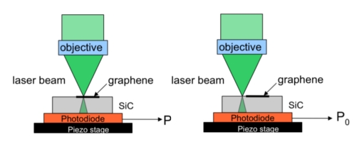
In this way, the power transmitted through the sample and the associated micro-Raman spectrum are measured at the same time, on the same point, using the same laser beam as a probe.
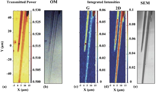
Transmission map and Raman integrated intensities maps (G and 2D bands) are compared to optical microscopy (OM) and scanning electron microscopy (SEM) images. We can clearly observe that the transmitted power is weaker through the two FLG ribbons shown on these maps because the absorptance of the graphene increases proportionally with its thickness (1.2 % of the incoming light is absorbed per graphene sheet on SiC substrates). The spectra corresponding to this two neighbouring ribbons are shown in the following figure.
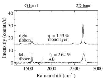
FLG’s spectra are obtained by subtracting a SiC reference. The combination of microtransmission measurements with microRaman spectroscopy allows to identify without any ambiguity that the left ribbon corresponds to a Bernal (AB) stacked graphene bilayer, and the right to a graphene monolayer.
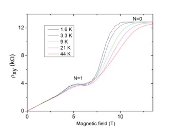
Transport properties of epitaxial graphene on SiC. Electrical measurements performed on graphene reveal the extremely unusual nature of the carriers. The value of the conductivity at the Dirac point, which does not correspond to its theoretical expectation, is an open problem, as well as the asymmetry in the conductivity of electrons and holes. Low magnetic fields studies reveal the presence (or the absence !) of quantum inferences, leading to positive and negative magnetoresistances. The positive magnetoresistance (also known as weak antilocalization) is a direct sizable consequence of the absence of backscattering for the Dirac particles. In high magnetic fields, in the quantum limit, Landau levels form at energies following a law in B1/2 - the first Landau Level being stuck at the Dirac point. At even higher fields, some evidences for unusual fractional quantum Hall effect (with anomalous fractions) have been reported. These unfamiliar characteristics are far from being completely understood or explored. Nevertheless, applications already are targeted : metrology (as the Quantum Hall effect in graphene persists up to room temperature) ; TeraHertz generation ; gas sensors ; supercapacitors ; even tactile touch screens.
Currently a large part of our activity is focussed on the physical properties of epitaxial graphene layers. How large can be the layers ? How they interact with the substrate ? Device fabrication largely uses clean room facilities. Transport measurements are routinely done in large magnetic fields (up to 14T) in a large range of temperatures (50mK-300K). We have at disposal four variable temperature insets (1.5K- 300K), one He3 inset, a small He3/He4 dilution unit, resistive magnets (0.3T ; 1T) ; cryostats shipped with superconducting magnets (3T ; 9T and 14T).
Funding :
ANR–07-Blanc-0161 “GraphSiC”
GDR C-Nano GSO
GDR GNTC
ANR Pnano “Graphonics”
ITN Netfisic
References :
Probing the electrical anisotropy of multilayer graphene on the Si face of 6H-SiC
B. Jouault, B. Jabakhanji, N. Camara, W. Desrat, A. Tiberj, J.-R. Huntzinger, C. Consejo, A. Caboni, P. Godignon, Y. Kopelevich, J. Camassel
Physical Review B 82, 085438 (2010)
Anisotropic growth of long isolated graphene ribbons on the C face of graphite-capped 6H-SiC
N. Camara, J.-R. Huntzinger, G. Rius, A. Tiberj, N. Mestres, F. Perez-Murano, P. Godignon, J. Camassel,
Physical Review B 80, 125410 (2009)
Electrical properties of the graphene/4H-SiC (0001) interface probed by scanning current spectroscopy
S. Sonde, F. Giannazzo, V. Raineri, R. Yakimova, J.-R. Huntzinger, A. Tiberj, J. Camassel
Physical Review B 80, 241406 (2009)
Selective epitaxial growth of graphene on SiC
N. Camara, G. Rius, J.-R. Huntzinger, A. Tiberj, N. Mestres, P. Godignon, J. Camassel
Applied Physics Letters 93, 123503 (2008)
Early stage formation of graphene on the C face of 6H-SiC
N. Camara, G. Rius, J.-R. Huntzinger, A. Tiberj, L. Magaud, N. Mestres, P. Godignon, J. Camassel
Applied Physics Letters 93, 263102 (2008)
Growth of monolayer graphene on 8° off-axis 4H–SiC „000–1… substrates with application to quantum transport devices
N. Camara, B. Jouault, A. Caboni, B. Jabakhanji, W. Desrat, E. Pausas, C. Consejo, N. Mestres, P. Godignon, and J. Camassel
Applied Physics Letters 97, 093107 (2010)
Current status of self-organized epitaxial graphene ribbons on the C face of 6H–SiC substrates
N. Camara, A. Tiberj, B. Jouault, A. Caboni, B. Jabakhanji, N. Mestres, P. Godignon, J. Camassel
Journal of Physics D : Applied Physics 43, 374011 (2010)
