

Rechercher


Accueil > La Recherche > Axes & Equipes > Physique Appliquée > Transport Quantique & Nouveaux Systèmes 2D > Thème : Nanostructuration des Matériaux
CIS based Photovoltaic Structures
publié le , mis à jour le
The current photovoltaic technology is mostly based on silicon. However efficiencies are already relatively optimized and no drastic increase of the efficiency of silicon based devices is to be expected, at least from the present common device concepts. Metallurgy of silicon is also a heavy technology, with a power and carbon balance that can be questioned. As a result, there is a lot of room for new materials.
Alloy semiconducting compounds offer many possibilities to design efficient photovoltaic devices. A quaternary like CuInxGa(1-x)Se2 (CIGS) allows for the realization of devices whose efficiencies are similar to silicon based cells, but with a projected cost per watt among the lowest in a near future.
Empirical approaches have permitted to realize good commercial devices, however a better understanding of the basic physics of the material growth, the role and nature of defects, as well as of the physical properties of CIGS based heterojunctions will pave the way towards more efficient devices, expanding their potential and use.
Our project aims at studying the growth mechanisms and material properties of CIS based thin films, and the relations between structure and physical properties.
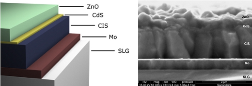
We implement together the specific growth technologies for each material involved in the photovoltaic device :
– the absorber consisting of the CuInSe2 based epilayer is grown by Physical Vapor Deposition (PVD) in a Molecular Beam Epitaxy (MBE) system ;
– the CdS buffer layer is deposited by chemical bath deposition (CBD) ;
– the ZnO window layer is obtained by electrochemical deposition (ED).
The Mo contact layer is deposited on soda lime glass substrates by sputtering.
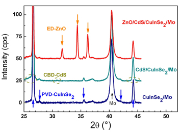
The thin films growth mechanisms are studied alone independently of the whole structure, as well as being a part of it.
Both thin films and structures are thoroughly characterized by using optical, electrical and structural characterizations.
