

Rechercher


Accueil > La Recherche > Axes & Equipes > Physique Appliquée > Transport Quantique & Nouveaux Systèmes 2D > Thème : Composants et Capteurs
Silicon Carbide
publié le
The topic of Silicon carbide (SiC) is due to a long term collaboration with National and international University and Industries. SiC is an attractive material for developing high power devices, owing to its superior properties. However, the commercialization of 4H-SiC high voltage diodes has been hampered by the degradation problem of their forward I-V characteristics. This effect is associated with the presence of stacking faults (SF) in the material. Faults change the stacking sequence of the 4H polytype and result in quantum wells of a different polytype, for example cubic polytype (3C-SiC)), a few manometers, in a matrix of 4H-SiC. Optical techniques, low temperature photoluminescence (LTPL), LT-micro-Photoluminescence (μ-LTPL), cathodoluminescence and micro-Raman, have been combined to highlight and explore the SFs in 4H-SiC samples. For the first time, the screening of the internal electric field by free carriers has been identified. More recently, high-resolution transmission electronic microscopy (HR-TEM) measurements (Aristotle University of Thessaloniki) confirmed the structure and size of these nano-defects. The experimental results are correlated with theoretical calculations and developed in the thesis of Robert Teddy (2006-2009).
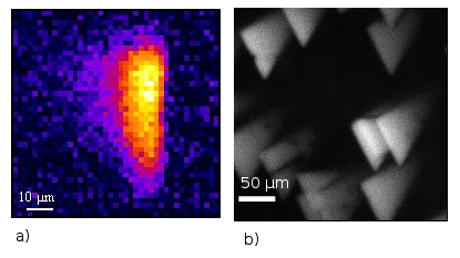
Because of our expertise on stacking faults, we lead the work package dedicated to this subject in the ANR project SiC-VHVD, started in January 2009, which groups together different laboratories and company (AMPERE, LMI, ISL and GES). The aim of this project is the design, the realization of silicon carbide high-voltage, 10 kV and with a final target of 15 kV type converters, compact, reliable and economically attractive for electrical distribution the market. In a first time and in collaboration with Subcontractor Linkoping, we have shown by LTPL and HR-TEM measurements that 3C-like zigzag faults can also exist in 4H-SiC and evidence the importance of carefully selecting substrates for high power device applications. In a second time, we have investigated the result of epitaxial growth performed on full 3” 4H-SiC substrates by Subcontractors LIU/IFM (Linkoping) in order to realize active device layers. To perform photoluminescence investigations at 2K, a new set-up was used. The set-up permits to investigate 4-inch sample at low temperature. On both samples a LTPL mapping was done, scanning with steps of 1 cm.
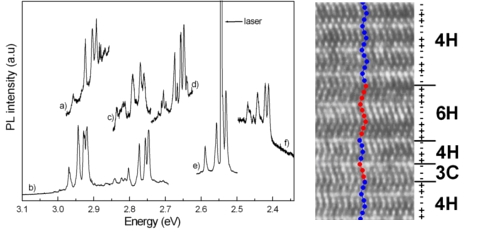
Stability problem in the 4H-SiC polytype make polytype 3C-SiC very attractive. Following Europeans projects SOLSIC and FLASIC, the scientific community has federated under a Marie Curie RTN network : “MANSIC” (2007-2010). The aim objective is to develop a line of components in 3C-SiC substrate components, one being the technological development of crystal size and quality compatible with the needs of the microelectronics especially in 3C-SiC. The spectroscopy measurements (LTPL and Raman) have revealed the polytype, doping and thickness of the first 3C-SiC materials developed on hexagonal substrates, according to the different growth techniques used by different partners network of 3C-SiC on α-SiC substrates.
For the next years, the crucial role of surface and interfaces especially if the components are used in harsh environments and under extreme conditions is in the focus. The aim of the ITN NetFISiC, starting in 2011, is the improvements of SiC devices are expected to come from a better control of metal/SiC (e.g. for Schottky diodes) and SiO2/SiC (e.g. for MOSFET) interfaces. This shall lead to improved channel mobility, without losing the outstanding blocking properties of SiC, and also to an extended range for the use of contact such as Schottky type. Targeted applications are high temperatures sensors, high power and/or high voltage devices, in addition to more innovating devices which need specific material development (other polytypes, graphene).
Collaboration/Contract :
ANR VHVD-SiC
MRTN-CT-2006-°35735 Marie-Curie MANSIC 2007-2010
ITN NetFISiC (2011-2014)
